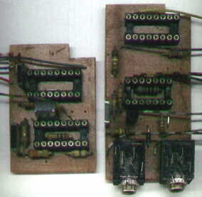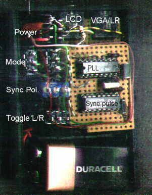
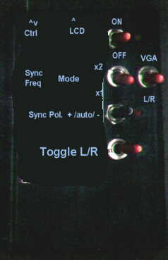
Now, finally, some pictures of the device (just to prove that I did more than paperwork). Please excuse for the poor quality, but they were scanned with my olde handy scanner, straight from the hardware.
First, pictures of the inside and outside of my first prototype, which is almost identical to the V1.0 PCB design. Not too much to see, I must admit, except that the thing is really packed. The dark reddish spot above 'Power' is the Tantal cap, below 'LCD' you can imagine the extra Z-diode and resitor to clamp the Vsync output to TTL level, which have been added on the V1.1 PCB.
The front panel mainly shows the switch functions. To be honest, the real device only has an ugly hand-written sticker on it, which I wiped out and added the captions in the scanned picture for clarity. to the right of the ON/OFF switch you should try to imagine the power LED; to the right of the 'Sync Pol.' and 'Toggle L/R' switches I had placed two spare LEDs, which were never really used (but look better than holes).


Finally, for now, the two PCBs of Rev 1.0, almost ready to go, except for the ICs and the vertical wires to connect the two boards.
